Ensure Proper Stackup Design in Rigid Flex PCBs
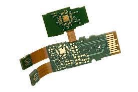
Rigid Flex PCBs
For a printed circuit board to function properly, its copper layers must be arranged correctly. This is especially true for rigid-flex circuits, which incorporate both stiffeners and flex sections. Rigid-flex PCBs are used in a variety of applications, including wearable electronics such as fitness and health monitors, foldable devices that can be worn and stored as part of clothing, conformal heating elements, and medical devices. To ensure that these devices meet their design requirements and are manufacturable, it is critical to plan the flex and rigid-flex layer stacks in advance of production.
The correct stackup configuration in a rigid flex circuits is dependent on a number of factors, such as signal integrity, flexibility requirements, and manufacturing constraints. The right combination of materials can offer an optimal mix of rigid and flexible sections, which is vital for the proper operation and reliability of a device.
A key issue to consider is the flex section’s flexibility and bend radius. This is important to ensure that the device can accommodate mechanical stress, reduce failure rates, and avoid bending fatigue. To address this, a number of techniques are used in the design process. For example, traces can be routed using teardrops, which expand the copper area and provide reinforcement. It is also important to minimize the number of rigid and flex layers in the flex section. Doing so will improve the material’s resilience and help to prevent cracking or fatigue.
Ensure Proper Stackup Design in Rigid Flex PCBs
Moreover, the thickness of the flex layer must be considered. Too thick a flex section can inhibit bending and flexing, while too thin can create an unstable design. To avoid this, a number of rigid and flex layers are typically staggered to achieve an appropriate balance. The rigid sections should also include reinforcing layers to maintain stiffness and allow a large enough space for components.
Additionally, a coverlay is often placed over the top of the copper layers to protect them from oxidation. This is an important step because oxidation can cause failure in rigid-flex designs. However, the thickness of this layer should be minimized to keep it from obstructing conductive pathways or preventing proper thermal management.
The most important consideration when planning a rigid-flex stackup is to consult with the PCB manufacturer. This will ensure that the flex and rigid-flex layers can be manufactured as intended and that they will be compatible with the manufacturing process. In addition, working with the CM will also help to identify any issues during the DFM review process and make it easier for the designer to resolve them.
To ensure that your rigid-flex PCB meets all its design requirements, you need to use a powerful PCB design platform. Altium Designer offers a single, unified environment that integrates routing, layer stackup, and design rule checking into one intuitive interface. Moreover, it provides powerful CAD tools, an ultra-accurate 3D viewer, and customizable routing and via features. This gives you everything you need to take your flex or rigid-flex design from conception to production.